semiconducting mazes
Okay, so this is mostly a bike blog, but since I got a new job in October, my time for riding has dropped off substantially. I'm trying to ride into work more often: once to twice per week would be good. But it's 42 miles one-way, so I've got to "make time" for that to happen.
Anyway, in my job, one of the products I use is a structure generator for semiconductor device modeling. So, for example, I can build models for field-effect transistors, bipolar junction transistors, p-i-n diodes, photo-detectors, light-emitting diodes, even static random access memory cells and other small circuits. Fun stuff, really. The models do a remarkably good job of matching reality, even though the reality of semiconductors can be fairly complex.
But when I found myself home sick with a bad cold, between naps I needed an activity to keep myself occupied. It was a good exercise to reacquaint myself with Scheme, the scripting language used by the structure editor. My Scheme was rusty, to say the least. Memories of 6.001 in my distant past.
And the best way to learn a computer language is to do an exercise, and since my job is modeling semiconductor devices, I should model a semiconductor device. But I was feeling poorly, and needed something to cheer myself up, and yet another FinFET simulation, for example, wasn't going to do that.
If Scheme has any strengths, it's in linked lists and recursion. And when I think linked lists and recursion, I think of mazes. From an early age I was fascinated with mazes. The labyrinth scene in The Shining, for example, still haunts me when I think about it.

close-up of model of the maze, from The Shining by Stanley Kubrik. The algorithm described here would need to be slightly modified to create this one, since it has loops (pairs of nodes connected by multiple paths).
So I set for myself the task of simulating a semiconductor maze. The thing here is that if you attach an electrode to the starting square and another to the goal square then apply, in simulation, a potential difference, current should almost instantly flow between the two. In other words, the maze will be solved. Would the simulator be able to solve the maze?
Well, the answer is it is, and remarkably well. Here's a plot of the current density through a simulated maze of doped Silicon, with an impurity concentration of 1 million arsenic atoms per cubic micrometer, enough to turn the semioconducting silicon into a decent conductor:

And here's another with more squares:
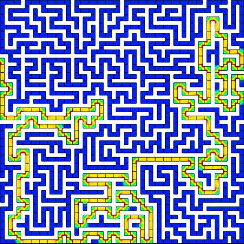
In each case a positive potential was applied to the left, causing current to flow to the right. Current density is indicated by color: red is the most current, blue is no current. White in the plot is "nothing": electrons can't go there (this isn't quite the same as "vaccuum", which I also could have modeled, but it's computationally quicker and mathematically similar to treat the walls of the maze as impermittable nothingness). The current flows only through the maze solution. Since the current was carried by electrons, this means the electrons, which are negatively charged, flow from right to left. They solve the maze backwards, you might say, although from a simulation perspective the direction doesn't matter.
You can even see the current cutting corners. When going straight, it spreads out to use the full width of the Si region. But when it turns a corner, it crowds to the inside to shorten the path.
So how did I create the maze? The algorithm, which is well-established, is simple. I start with a list of nodes plus a "stack" in which I can access only the top element. Basic actions with stacks include "pushing" an element onto the stack and "popping" the top element off the stack.
The nodes are each defined in terms of their neighbors. Neighbors can be either connected or disconnected, but initially each node has all of its neighbors disconnected.
I start with one random node on the left side of the maze. I put the number associated with that node onto the stack. Then I begin my process:
That's it! Very simple. The algorithm doesn't care where nodes are located or how they're laid out. The maze could be 2-dimensional, 3-dimensional, or even 4-dimensional. If 2-dimensional, it could be laid out in a square, as hexagons, as triangles, or as irregularly shaped elements. The maze is really a very general concept. It's really just a way of connecting a constrained network such that each element is connected to each other element by exactly one path.
A side-effect of this algorithm is, if you begin the process with the start node at the bottom of the stack, once the goal node is at the top of the stack (eventually it has to be if the maze has a solution), the stack contains the solution, from bottom to top. My code marks the elements of the stack with a number sequence indicating those nodes to be part of the solution, and in what order. However, this isn't relevant to this work: the solutions shown here were generated by the electron transport modeling in the semiconductor device modeler.
But once the abstract maze is connected, it needs to be mapped to "real space" for the simulation. So using the constructor functions in the structure editor, I defined polygons for each node such that the node was connected to the appropriate neighbors. Then I defined the semiconductor properties for the interconnected region, specified which models I wanted, and ran the simulation. Actually, constructing the maze took the most computer power. Solving it was quick: well under a minute for the larger of the two mazes shown here.
So all good fun. And it was effective at improving my Scheme skills. After this, designing my normal semiconductor device structures seemed simple in comparison.
Anyway, in my job, one of the products I use is a structure generator for semiconductor device modeling. So, for example, I can build models for field-effect transistors, bipolar junction transistors, p-i-n diodes, photo-detectors, light-emitting diodes, even static random access memory cells and other small circuits. Fun stuff, really. The models do a remarkably good job of matching reality, even though the reality of semiconductors can be fairly complex.
 |
| Knights of the Lambda Calculus |
And the best way to learn a computer language is to do an exercise, and since my job is modeling semiconductor devices, I should model a semiconductor device. But I was feeling poorly, and needed something to cheer myself up, and yet another FinFET simulation, for example, wasn't going to do that.
If Scheme has any strengths, it's in linked lists and recursion. And when I think linked lists and recursion, I think of mazes. From an early age I was fascinated with mazes. The labyrinth scene in The Shining, for example, still haunts me when I think about it.
close-up of model of the maze, from The Shining by Stanley Kubrik. The algorithm described here would need to be slightly modified to create this one, since it has loops (pairs of nodes connected by multiple paths).
So I set for myself the task of simulating a semiconductor maze. The thing here is that if you attach an electrode to the starting square and another to the goal square then apply, in simulation, a potential difference, current should almost instantly flow between the two. In other words, the maze will be solved. Would the simulator be able to solve the maze?
Well, the answer is it is, and remarkably well. Here's a plot of the current density through a simulated maze of doped Silicon, with an impurity concentration of 1 million arsenic atoms per cubic micrometer, enough to turn the semioconducting silicon into a decent conductor:
And here's another with more squares:
In each case a positive potential was applied to the left, causing current to flow to the right. Current density is indicated by color: red is the most current, blue is no current. White in the plot is "nothing": electrons can't go there (this isn't quite the same as "vaccuum", which I also could have modeled, but it's computationally quicker and mathematically similar to treat the walls of the maze as impermittable nothingness). The current flows only through the maze solution. Since the current was carried by electrons, this means the electrons, which are negatively charged, flow from right to left. They solve the maze backwards, you might say, although from a simulation perspective the direction doesn't matter.
You can even see the current cutting corners. When going straight, it spreads out to use the full width of the Si region. But when it turns a corner, it crowds to the inside to shorten the path.
So how did I create the maze? The algorithm, which is well-established, is simple. I start with a list of nodes plus a "stack" in which I can access only the top element. Basic actions with stacks include "pushing" an element onto the stack and "popping" the top element off the stack.
The nodes are each defined in terms of their neighbors. Neighbors can be either connected or disconnected, but initially each node has all of its neighbors disconnected.
I start with one random node on the left side of the maze. I put the number associated with that node onto the stack. Then I begin my process:
- If the stack is empty, I'm finished. The maze is done.
- If the top node on the stack has any neighbors which have as yet no connections, then pick one at random, connect the top node in the stack with that randomly chosen neighbors, put that neighbor on the top of the stack, and repeat.
- On the other hand, if the top node in the stack has no unconnected neighbors (neighbors which have no connections, to that node or to another node), then pop the stack and repeat.
That's it! Very simple. The algorithm doesn't care where nodes are located or how they're laid out. The maze could be 2-dimensional, 3-dimensional, or even 4-dimensional. If 2-dimensional, it could be laid out in a square, as hexagons, as triangles, or as irregularly shaped elements. The maze is really a very general concept. It's really just a way of connecting a constrained network such that each element is connected to each other element by exactly one path.
A side-effect of this algorithm is, if you begin the process with the start node at the bottom of the stack, once the goal node is at the top of the stack (eventually it has to be if the maze has a solution), the stack contains the solution, from bottom to top. My code marks the elements of the stack with a number sequence indicating those nodes to be part of the solution, and in what order. However, this isn't relevant to this work: the solutions shown here were generated by the electron transport modeling in the semiconductor device modeler.
But once the abstract maze is connected, it needs to be mapped to "real space" for the simulation. So using the constructor functions in the structure editor, I defined polygons for each node such that the node was connected to the appropriate neighbors. Then I defined the semiconductor properties for the interconnected region, specified which models I wanted, and ran the simulation. Actually, constructing the maze took the most computer power. Solving it was quick: well under a minute for the larger of the two mazes shown here.
So all good fun. And it was effective at improving my Scheme skills. After this, designing my normal semiconductor device structures seemed simple in comparison.


Comments